Integrating VERA.
Updated 2 April 2026: Corrected stale links.
Updated 23 December 2025: Removed reference to ‘On WSL’ documentation.
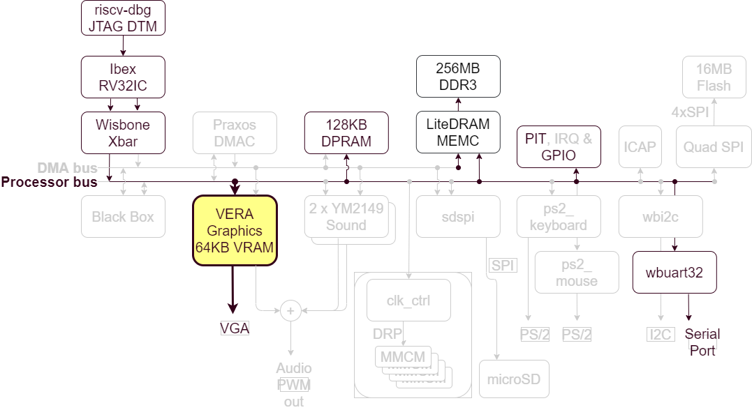
VERA in the BoxLambda Architecture.
Recap
This is a summary of the current state of affairs for BoxLambda. We have:
- An Ibex RISC-V core, Wishbone shared bus, timer, two GPIO ports, UART core, and internal memory.
- DDR3 external memory access through the Litex Memory Controller.
- OpenOCD-based Debug Access, both on FPGA and Verilator.
- Test builds running on Arty-A7-35T, Arty-A7-100T, and Verilator.
- A Picolibc-based standard C environment for software running on the Ibex RISC-V core.
- A Linux CMake and Bender-based RTL build system.
- Automated testing on Verilator.
In my previous post, I analyzed the internal structure and operation of the VERA (Versatile Embedded Retro Adapter) graphics pipeline. In this post, I focus on the modifications needed to make the VERA core a suitable component for a 32-bit Wishbone-based SoC. Specifically, BoxLambda.
VERA Modifications
The original VERA implementation is a standalone FPGA controlled by an 8-bit microprocessor via a low-speed 8-bit external bus. Certain modifications in the VERA code base are necessary to be able to fit the VERA core as a component into BoxLambda’s SoC. The subsections below highlight the implemented changes.
50MHz Core Clock Frequency
BoxLambda’s system clock frequency is 50MHz. It would be convenient to run the VERA core at that same speed. As it turns out, that works just fine. I didn’t run into any timing closure issues when synthesizing the core at 50MHz. For those parts of the core that need to run at the 25MHz pixel clock frequency (composer, video_vga), I introduced a toggling clock enable signal (clock enables are preferred over clock dividers).
Running the VERA core at 50MHz has the additional benefit of doubling the bandwidth of the VRAM bus. That’ll come in handy to absorb the impact of the VRAM scheduling and Sprite Rendering changes introduced below.
Wishbone Interface
The 8-bit asynchronous external bus is replaced with a pipelined Wishbone slave interface. The interface has a 32-bit data port, 4-byte lane enables, and a 17-bit word-addressed address port.
Generic Single Port RAM
The original VERA VRAM code uses a memory primitive, SP256K, that is specific to Lattice FPGA devices. I replaced the SP256K instances with instances of a generic Single Port RAM module that, in theory, should work well across a whole range of FPGA devices. Having said that, I have only been testing the modifications on Verilator and Arty A7.
Configurable VRAM Size
BoxLambda currently supports two FPGA configurations: The Arty-A7-35T and the Arty-A7-100T. I have to reduce VERA’s VRAM size to 64KB to be able to fit it into the small memory footprint of the Arty-A7-35T, but I want to leave it at 128KB for the bigger Arty-A7-100T. To handle this, I added a VRAM_SIZE_BYTES parameter to the top-level module and propagated it down to main_ram_generic, the module where the memory is instantiated.
The maximum value of VRAM_SIZE_BYTES is 131072 (128K). I have only tested values 65536 (64K) and 131072. 65536 is the default value for the Arty-A7-35T and Verilator. 131072 is the default for Arty-A7-100T.
Memory Mapped Access to VRAM, Palette RAM and Sprite Attribute RAM
The original VERA VRAM access method is geared towards an external 8-bit microcontroller. This pretty much made indirect access (with benefits such as auto-increment/decrement) a necessity. The wide address range of the Wishbone interface, combined with BoxLambda’s 32-bit RISCV processor removes this necessity. In such a configuration, it makes more sense to offer a straightforward memory-mapped interface to VRAM, Palette RAM, and Sprite Attribute RAM.
I removed the indirect memory access methods and created the following memory-mapped address ranges:
| Address Range | Description | Access |
|---|---|---|
| 0x10100000 - 0x10100100 | VERA Registers | Read/Write |
| 0x10101000 - 0x10101400 | Sprite attributes | Write Only |
| 0x10102000 - 0x10102200 | Palette | Write Only |
| 0x10140000 - 0x10160000 | Video RAM (128KB) | Read/Write |
Note:
- The above addresses are absolute, as seen by the RISCV processor. The VERA core’s base address is 0x10100000.
- The Video RAM address range depends on the amount of Video RAM set by the VRAM_SIZE_BYTES macro. The range 0x10140000-0x10160000 corresponds to a VRAM_SIZE_BYTES setting of 131072 (128K).
Time Slot Scheduled Access to VRAM
Four ports are accessing VRAM: two Layer Renderers, the Sprite Renderer, and the CPU. The original VERA code uses a priority scheduler to decide which port gets access when two or more ports are competing for access. The CPU port had the highest priority, then the Layer Renderers, and finally the Sprite Renderer. However, the high-speed, memory-mapped Wishbone interface makes it all too easy for the CPU to oversubscribe the VRAM bus and starve the other ports of bandwidth. This would result in tearing artifacts and other rendering errors. To avoid this issue, the priority scheduler is replaced with a time slot scheduler. There are four equal time slot beats. Each port is assigned one slot during which it can access VRAM. The duration of a time slot is one clock cycle.
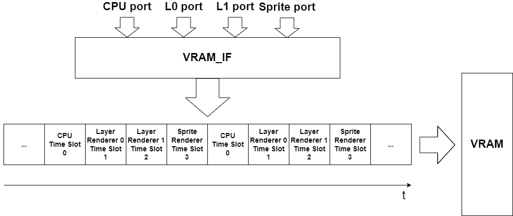
Time Slot Scheduled VRAM Access.
With this mechanism, bandwidth utilization on one port does not have any impact on any of the other ports. A port that tries to use more than its share of the bus bandwidth is stalled. In practice, the only port where this can happen is the CPU port.
Sprite Banks
One nice consequence of the time slot scheduling is that the Sprites-per-Scanline limit no longer depends on the selected Layer Renderer modes. However, that limit also depends to some extent on the position of the enabled sprites in the Sprite Attribute Table. Each scanline, the Sprite Attribute Table is scanned front-to-back for enabled sprites. This takes time. As a result, if all enabled sprites are located towards the end of the table, the Sprites-per-Scanline limit is lower compared to having the same number of enabled sprites near the front of the table. This is undesirable. It goes against the grain of BoxLambda’s deterministic behavior requirement.
One way to avoid the issue is to conservatively reduce the Sprite ID maximum value to the Sprites-per-Scanline limit minus 1, i.e. when the limit is reached, the table is full and there is no front-of-table or back-of-table effect to consider. By running the VERA core at 50MHz, the largest number of sprites that can be guaranteed to be rendered completely on one scanline is 64. This is for 8-pixel-wide sprites. In other words, the highest Sprites-per-Scanline limit is 64, and Sprite IDs should be limited to the range of 0 to 63.
However, limiting the Sprite ID maximum value to 63 would mean that the upper half of the Sprite Attributes RAM is left unused. We could just cut the size of that RAM in half. Instead, I chose to create two banks of 64 sprite IDs. A bit in the VERA_CTRL register is used to select the active bank.
Sprite Banking may help with sprite multiplexing or animation: While one sprite bank is active, software can prepare the inactive bank’s entries and switch over at the right moment, triggered by a line_irq, for instance.
![]()
Double Buffering with Sprite Banks Example.
![]()
Sprite Multiplexing with Sprite Banks Example.
A Fixed Sprite-Pixels-per-Scanline Limit
The Sprites-per-Scanline limit is inversely proportional to the sprite width. That makes sense. It takes roughly twice as long to render a 16-pixel-wide sprite than an 8-pixel-wide sprite (See also Maximum number of Sprites per Scanline table in the Understanding VERA post). Conversely, the number of sprite pixels that can be rendered on a given scanline is relatively constant. With all of the above modifications implemented, this constant is 512 pixels, i.e. the Sprite Renderer can render a maximum of 512 sprite pixels on any scanline, guaranteed.
The original Sprite Renderer code kept track of rendering time to decide when to abort rendering, to avoid exceeding its time budget. I replaced that code with logic that keeps track of the number of sprite pixels rendered. When 512 sprite pixels are rendered, further sprite rendering is aborted for the given scanline.
![]()
Examples of the 512 Sprite Pixel Limit.
The above changes combined make it easier for a programmer to plan sprites. The programmer knows ahead of time exactly how many sprites of a given size he can have on the same scanline. This number is independent of the Layer Renderer settings and the VRAM loading by the CPU (or any other Wishbone bus master accessing VRAM, such as a DMA core).
32-bit friendly register access
I reshuffled the various bitfields in VERA’s register space for convenient access by a 32-bit CPU. Here is the modified register interface:
| Addr | Name | 31-12 | 11 | 10 | 9 | 8 | 7 | 6 | 5 | 4 | 3 | 2 | 1 | 0 |
|---|---|---|---|---|---|---|---|---|---|---|---|---|---|---|
| $00 | CTRL | - | - | - | - | - | - | - | - | - | - | - | - | SBNK |
| $04 | DC_BORDER | - | - | - | - | - | Border Color | |||||||
| $08 | IEN | - | - | - | - | - | - | - | - | - | - | SPRCOL | LINE | VSYNC |
| $0C | ISR | - | - | - | - | - | Sprite collissions | - | SPRCOL | LINE | VSYNC | |||
| $10 | IRQLINE | - | - | - | IRQ line | |||||||||
| $14 | SCANLINE | - | - | - | Scan line | |||||||||
| $18 | DC_VIDEO | - | - | - | - | - | - | Sprites Enable | Layer1 Enable | Layer0 Enable | - | - | Output Mode | |
| $20 | DC_HSCALE | - | - | - | - | - | Active Display H-Scale | |||||||
| $24 | DC_VSCALE | - | - | - | - | - | Active Display V-Scale | |||||||
| $28 | DC_HSTART | - | - | - | Active Display H-Start | |||||||||
| $2C | DC_HSTOP | - | - | - | Active Display H-Stop | |||||||||
| $30 | DC_VSTART | - | - | - | Active Display V-Start | |||||||||
| $34 | DC_VSTOP | - | - | - | Active Display V-Stop | |||||||||
| $40 | L0_CONFIG | - | - | - | - | - | Map Height | Map Width | T256C | Bitmap Mode | Color Depth | |||
| $44 | L0_MAPBASE | - | - | - | - | - | Map Base Address (16:9) | |||||||
| $48 | L0_TILEBASE | - | - | - | - | - | Tile Base Address (16:11) | Tile Height | Tile Width | |||||
| $50 | L0_HSCROLL | - | H-Scroll | |||||||||||
| $54 | L0_VSCROLL | - | V-Scroll | |||||||||||
| $80 | L1_CONFIG | - | - | - | - | - | Map Height | Map Width | T256C | Bitmap Mode | Color Depth | |||
| $84 | L1_MAPBASE | - | - | - | - | - | Map Base Address (16:9) | |||||||
| $88 | L1_TILEBASE | - | - | - | - | - | Tile Base Address (16:11) | Tile Height | Tile Width | |||||
| $90 | L1_HSCROLL | - | H-Scroll | |||||||||||
| $94 | L1_VSCROLL | - | V-Scroll | |||||||||||
All registers are 32-bit wide, but higher order bits 31-12 are currently not in use.
For a description of these registers, refer to the VERA Programmer’s Reference.
The VERA Wishbone Repo
The revised VERA repository is called vera_wishbone:
https://github.com/epsilon537/vera_wishbone
VERA Wishbone’s feature summary:
- 32-bit pipelined Wishbone slave interface.
- VGA output format at a fixed resolution of 640x480@60Hz (same as original VERA).
- Support for 2 layers, both supporting either tile or bitmap mode (same as original VERA).
- Support for 2 banks of 64 sprites. Guaranteed max. of 512 sprite pixels per scanline.
- Configurable Embedded video RAM size of up to 128kB.
- Palette with 256 colors selected from a total range of 4096 colors (same as original VERA).
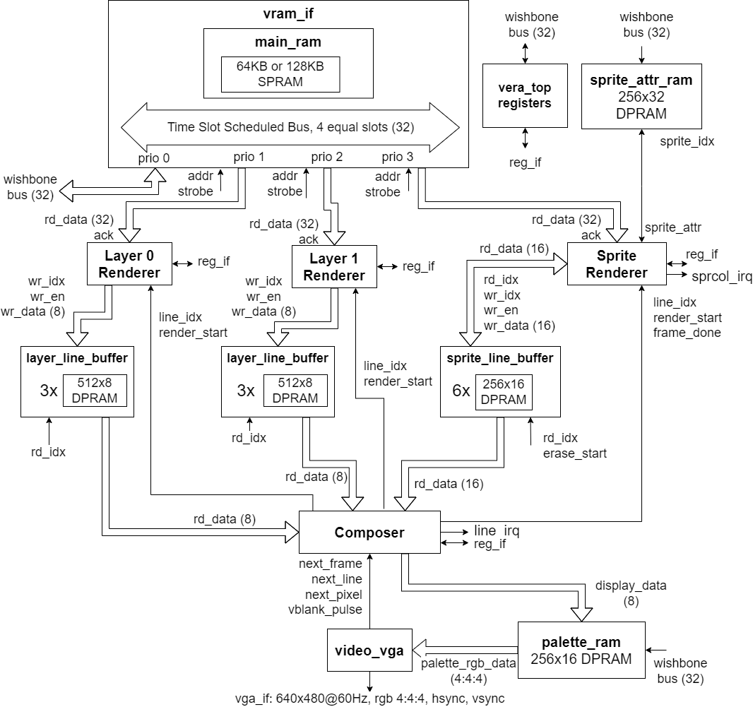
The VERA Wishbone Block Diagram.
The vera_wishbone top-level interface is straightforward:
module vera_top #(
	parameter VRAM_SIZE_BYTES=(128*1024) //Max. 128KB.
	)
  (
  input  wire       clk,
  input  wire       reset,

  //32-bit pipelined Wishbone interface.
  input wire [16:0]  wb_adr,
  input wire [31:0]  wb_dat_w,
  output wire [31:0] wb_dat_r,
  input wire [3:0]   wb_sel,
  output wire        wb_stall,
  input wire         wb_cyc,
  input wire         wb_stb,
  output wire        wb_ack,
  input wire         wb_we,
  output wire        wb_err,

  // IRQ
  output wire        irq_n,

  // VGA interface
  output reg  [3:0]  vga_r,
  output reg  [3:0]  vga_g,
  output reg  [3:0]  vga_b,
  output reg         vga_hsync,
  output reg         vga_vsync
  );
VERA Wishbone Test Builds
Vera_Standalone
The vera_standalone test project introduced in the previous post is still functional. It’s a Verilator simulation project containing just the VERA core and a test bench. The test bench has been updated to track the various modifications to the VERA core and it has been extended to support the rendering of the VGA output in a window using SDL.
Vera_standalone served its purpose of testing the VERA core and modifications pre-integration. Once the VERA core was integrated into the BoxLambda SoC, however, the vera_integrated test SoC project took over. I don’t intend to further maintain the vera_standalone project after I have applied the vera_integrated git label.
Location of the vera_standalone project: boxlambda/gw/projects/vera_standalone.
Vera_Integrated
boxlambda/gw/projects/vera_integrated contains a BoxLambda test SoC including the vera_wishbone core. As is the case with the vera_standalone build, the associated test bench will render the VGA output to a window using SDL. The test bench will also save a fully rendered frame as a file, so it can be compared against a reference frame for automated testing.
In the vera_integrated build, VERA is configured by a test program running on the Ibex RISCV processor that’s part of the test SoC. The test program communicates with the test bench over UART. This allows the test program to send test results to the test bench for automated testing. The test program focuses on the VERA core modifications discussed above:
- Wishbone read and write access to VERA registers and memories.
- Sprite Banking.
- The 512 sprite-pixels-per-scanline limit.
- The modified register interface.
- VRAM bus timeslot scheduling by verifying that Layer and Sprite Rendering are not affected by CPU load on VRAM.
For the Arty A7 build, the .xdc constraints file used by vera_integrated assumes that Diligent’s VGA PMOD is being used, i.e. the VGA signals are sent to PMOD ports JB and JC with the following pin layout:
| Pin | Description | Pin | Description |
|---|---|---|---|
| JB Pin 1 | R0 | JC Pin 1 | G0 |
| JB Pin 2 | R1 | JC Pin 2 | G1 |
| JB Pin 3 | R2 | JC Pin 3 | G2 |
| JB Pin 4 | R3 | JC Pin 4 | G3 |
| JB Pin 5 | GND | JC Pin 5 | GND |
| JB Pin 6 | VCC | JC Pin 6 | VC3V3 |
| JB Pin 7 | B0 | JC Pin 7 | HS |
| JB Pin 8 | B1 | JC Pin 8 | VS |
| JB Pin 9 | B2 | JC Pin 9 | NC |
| JB Pin 10 | B3 | JC Pin 10 | NC |
| JB Pin 11 | GND | JC Pin 11 | GND |
| JB Pin 12 | VCC3V3 | JC Pin 12 | VCC |
Try It Out
Setup
- Install the Prerequisites.
- Get the BoxLambda repository:
git clone https://github.com/epsilon537/boxlambda/ cd boxlambda - Switch to the vera_integrated tag:
git checkout vera_integrated - Set up the repository. This initializes the git submodules used and creates the default build trees:
./boxlambda_setup.sh
Vera_standalone on Verilator
- Build the vera_standalone project:
cd build/sim/gw/projects/vera_standalone make vera_standalone_sim - Execute the generated Verilator model:
./Vmodel - Vmodel opens a window in which the VGA output is rendered pixel-by-pixel. You should see the following frame appear:
Frame generated by vera_standalone Verilator model.
Vera_integrated on Verilator
- Build the vera_integrated project:
cd build/sim/gw/projects/vera_integrated make vera_integrated_sim - Execute the generated Verilator model:
./Vmodel - Vmodel opens a window where the VGA output is rendered pixel-by-pixel. You should see the following frame appear:
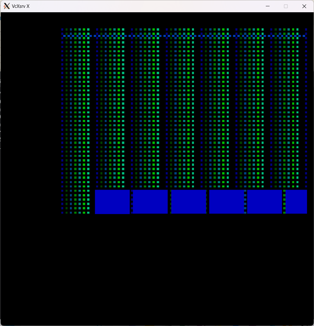
Frame generated by vera_integrated Verilator model.
The terminal window should look like this:

Vera_integrated Verilator model terminal window output.
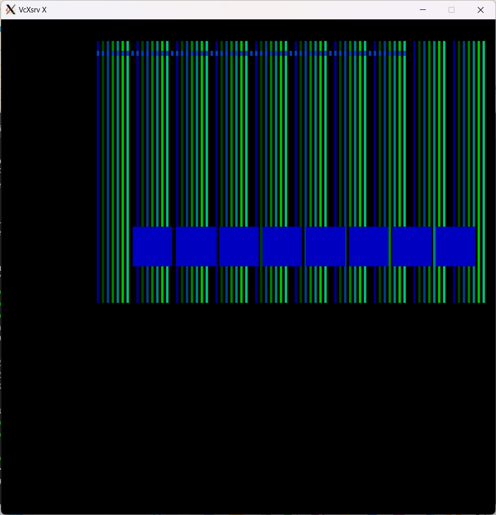
Vera_integrated on the Arty A7
- Hook up a VGA display to the Arty A7 PMOD ports JB and JC using Diligent’s VGA PMOD.
- Build the vera_integrated project in an Arty A7 build tree (arty-a7-35 or arty-a7-100):
cd build/arty-a7-35/gw/projects/vera_integrated make vera_integrated_impl - Download the generated bitstream file to the Arty A7:
make vera_integrated_load - The display should now show a bunch of colored squares. Here’s a picture of my setup. Apologies for the potato quality. It shows that I’m spending more on FPGA dev boards than on cameras.
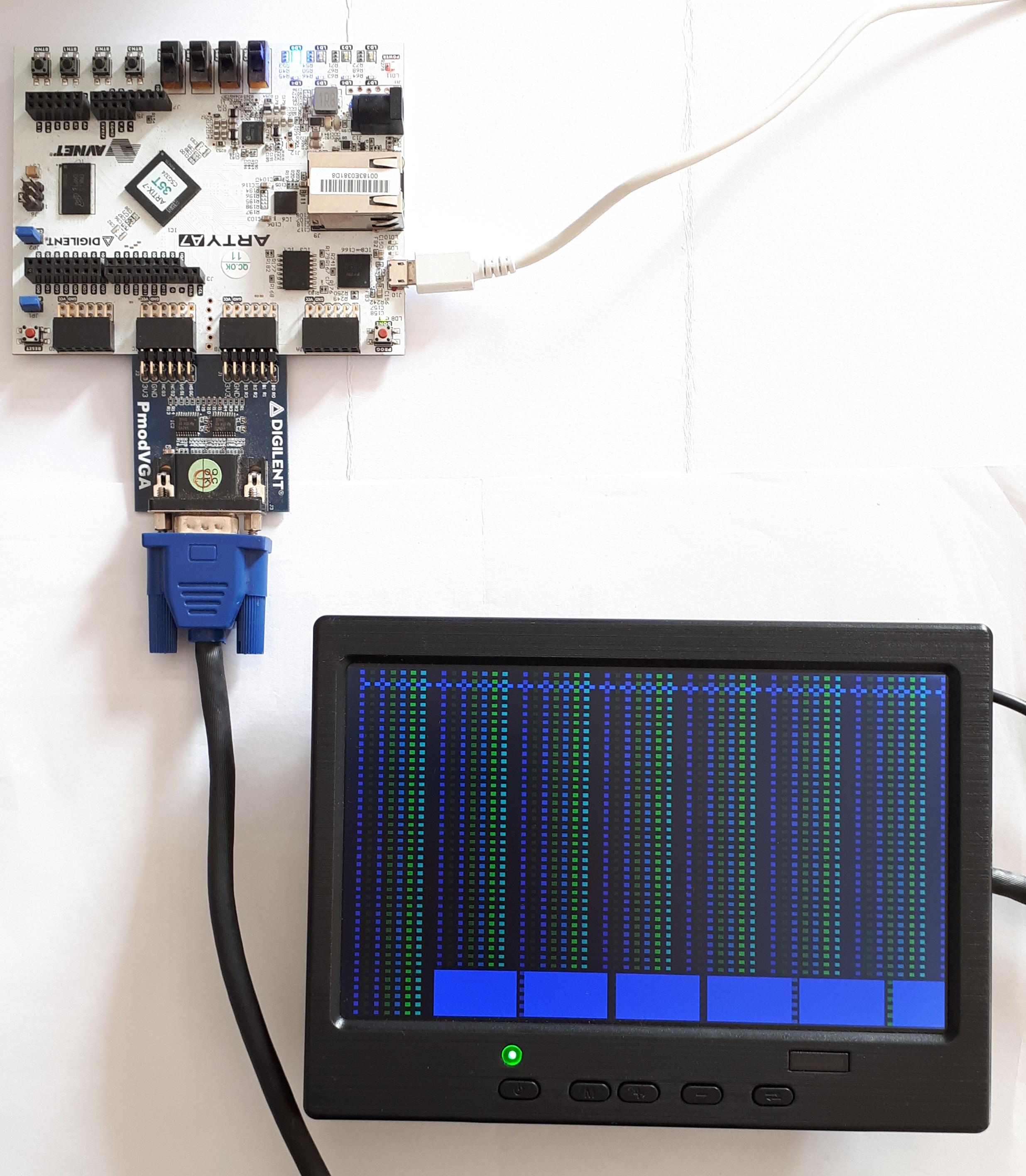
Arty A7 Setup for the vera_integrated Test SoC.
Conclusion
Having taken the time to study the original VERA’s internal structure and operation, identifying the necessary modifications needed to integrate the core into a 32-bit SoC was relatively straightforward. Most changes are implemented in the top-level module, vera_top. In this module, the Wishbone bus is terminated, the VERA registers are kept, and the memory-mapped access to the various RAMs is implemented. Key to the whole exercise is the Verilator simulation model of the VERA core and its ability to render the VGA output in a window.
In the next post, I would like to bring up the SD SPI controller and get a filesystem going. Thank you for reading. Please let me know what you think.