Understanding VERA.
Updated 2 April 2026: Corrected stale links.
Updated 13 March 2023: Parts of this article have been updated since the original post:
- Replaced the term Main RAM with VRAM.
- Added a Video RAM section.
- Added the FPGA device targeted by VERA.
- Indicated that collision detection is limited to Sprite-to-Sprite collision detection.
- Some rewording.
Frank van den Hoef’s VERA Versatile Embedded Retro Adapter, used by the Commander X16 project, is a standalone FPGA with an 8-bit external bus interface. I spent some time studying VERA’s Video Controller implementation, out of interest, and because I need a good understanding of VERA to be able to integrate it properly into the BoxLambda SoC.
Video Generator Features
VERA supports PSG Audio, PCM Audio, and a SPI Controller for storage, but I’ll be focusing on just the video generator aspect of VERA. Furthermore, I’ll focus on just the VGA data path, while VERA does support NTSC Composite, NTSC S-Video, and RGB video as well.
The VERA VGA video generator has the following features:
- Multiple output formats (VGA, NTSC Composite, NTSC S-Video, RGB video) at a fixed resolution of 640x480@60Hz.
- Support for 2 layers, both supporting either tile or Bitmap Mode.
- Support for up to 128 sprites.
- Embedded video RAM (VRAM) of 128KB.
- Palette with 256 colors selected from a total range of 4096 colors.
The above list is taken from VERA’s Programmer’s Reference. If you haven’t done so yet, it’s a good idea to go through that document. It’s brief and to the point. It’ll give you a good understanding of VERA’s capabilities and how it presents itself to a CPU.
The FPGA targeted by VERA is a Lattice ICE40UP5K. This FPGA has 5280 LUTs, 1024Kbit of SPRAM, and 120Kbit of EBR RAM.
Overview
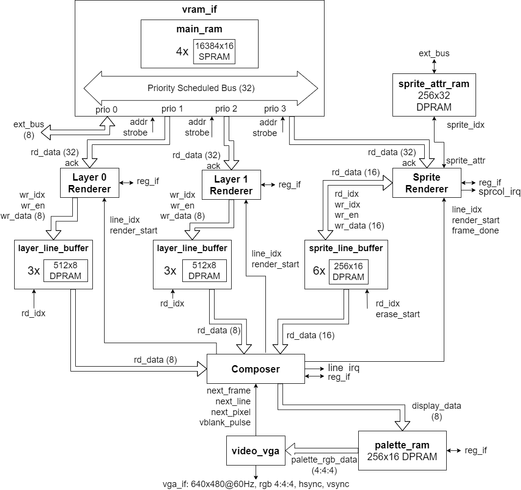
VERA Video Block Diagram.
This block diagram is a bit overloaded, but if you stare at it long enough, you’ll get a pretty good idea of how the VERA video datapath is working. The bigger arrows show the main data flow. The small arrows are control signals. The labels next to the arrowheads show what is being presented to the block at that point. E.g. the Composer presents a line_idx and render_start signal to the Layer 0 Renderer. Data path bus widths are indicated by a number between brackets.
The whole system operates at 25MHz, the 640x480@60Hz pixel clock rate.
The easiest way to understand what’s going on is by going through the diagram from bottom to top:
- The video_vga block generates the 640x480@60Hz VGA signal (RGB 4:4:4, Hsync and Vsync).
- The video_vga block pulls the pixel data from the Composer block. The 8-bit pixel data passes through the palette_ram to be converted to RGB 4:4:4.
- The Composer block in turn pulls the necessary data from three Line Buffers: one for each layer and one for sprites. The Composer and video_vga blocks operate at VGA pixel clock rate, i.e. 640 pixels worth of data flows when a scanline is being drawn. No data flows during horizontal or vertical retrace.
- The Line Buffers exist to give the renderers some leeway. The Layer Renderers, for instance, need to produce 640 pixels worth of data each scanline but they have 800 pixels worth of time to do so (the horizontal retrace time is ‘extra time’). For the Sprite Renderer, the numbers are a bit different, but the concept is the same.
- The renderers contain the bulk of VERA’s video generation logic. There are two identical Layer Renderer blocks and one Sprite Renderer. The Layer Renderers implement the different tile and Bitmap Modes, retrieve the necessary data from the vram_if block and store the rendered output data in their respective Line Buffers. The Sprite Renderer does the same thing for sprites.
- The vram_if block contains 128KB of embedded video memory and an arbiter. It has four ports: one for each renderer and one for the CPU (via the external bus).
Video RAM
The video RAM (VRAM) consists of four blocks of on-chip Single Port RAM. Each block holds 16384 16-bit words. A module named main_ram organizes these four blocks into a memory of 32768 32-bit words. A port-based priority scheduler inside the vram_if block arbitrates access to this 32-bit memory. The CPU/external bus has the highest priority, then the layer 0 renderer, the layer 1 renderer, and finally the sprite renderer, in that order.
The Composer
The Composer receives basic control signals from the video_vga block: next pixel, next line, next frame, vblank. It uses these signals for the following purposes:
- Generate control/timing signals towards the other blocks, e.g. line index, render start, frame done, sprite Line Buffer erase start.
- Keep track of the horizontal and vertical screen position counters, both regular and scaled.
- Generate line IRQs.
- Determine the active area of the screen, where the border isn’t shown.
- Compose the display, reading out the pixel data from the three Line Buffers.
The Layer Renderer
The Layer Render’s implementation is, conceptually at least, reasonably straightforward:
- Depending on the scanline index and the current position in the Line Buffer, it retrieves the appropriate map entry from VRAM (assuming Tile Mode).
- It retrieves the corresponding tile pixel data, also from VRAM.
- It writes out the pixel data to the next few positions in the Line Buffer.
Steps 1 and 2 are always sequential, but as much as possible they overlap with step 3, i.e. while pixel data is being rendered out to the Line Buffer, new map and/or tile data is being retrieved from VRAM.
Below you see the waveform of the Layer Renderer operating in 8bpp Tile Mode, 8 pixel wide tiles. One full FSM (Finite State Machine) cycle is shown, i.e. the pattern between the two vertical cursors is repeating. You can see the VRAM reads (buf_strobe and bus_ack) happening in parallel with the Line Buffer writes (lb_wridx_r). You can also see how the Renderer FSM cycles through its states (fetch map, wait fetch map, fetch tile, wait fetch tile, render, etc.).
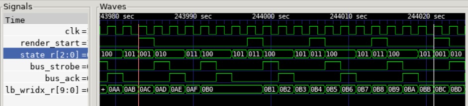
Layer Rendering Waveform.
Other Layer Renderer Responsibilities
Other responsibilities of the Layer Renderer include:
- Bitmap Mode: Simpler than Tile Mode, but more expensive in terms of required memory resources. In Bitmap Mode, VRAM holds a frame buffer.
- Handling of vertical and horizontal scrolling.
- Handling of the different colors-depths: 8bpp, 4bpp, 2bpp, 1bpp.
- Handling of the different tile widths and heights.
- Tile V-flip and H-flip.
The Layer Line Buffer
The Layer Renderer has an 8-bit write-only interface to its Line Buffer. The Line Buffer contains 8 bits per entry. One entry corresponds to one pixel. The Layer Line Buffer implements a double buffering scheme: While the renderer is writing out one scanline, the Composer is reading out the other line. When they are done with the respective scanlines, they switch places.
The Sprite Renderer
The Sprite Renderer’s operation is a bit more complicated:
- The Sprite Attribute RAM is scanned front-to-back to find the next sprite ID that is active on the current scanline.
- When an active Sprite has been found, its pixel data for the current scanline is retrieved from VRAM.
- The pixel data is written out to the correct positions in the Line Buffer. That means there may be multiple overlapping writes into the Sprite Line Buffer. The Sprite Line Buffer is written in Sprite ID order, at the position determined by the sprite’s X-coordinate.
The sequence of scanning the sprite attribute RAM, retrieving sprite pixel data, and rendering it out to the Line Buffer is entirely sequential. There is no pipelining.
In the waveform below, you can see two sprites getting rendered out on a scanline: sprite ID 4 at position 192, and sprite ID 5 at position 256. The two sprites have 8bpp color depth and are 8 pixels wide. You can see that, for each sprite, two VRAM read operations are performed (bus_strobe and bus_ack signals), and 8 entries are accessed in the Sprite Line Buffer (linebuf_idx_r).
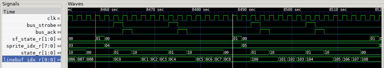
Sprite Rendering Waveform.
Other Sprite Renderer Responsibilities
Other responsibilities of the Sprite Renderer include:
- Decoding and handling of sprite attributes: color-depth, width, height, z-depth, and collision mask.
- Sprite-to-Sprite Collision Detection.
- Handling pixel transparency.
The Sprite Line Buffer
The Sprite Line Buffer contains 16 bits per entry. One entry corresponds to one pixel. Each entry contains the sprite pixel’s collision data and z-value (layering depth relative to layers 0 and 1), along with the pixel data. The Sprite Renderer’s collision handling logic has to be able to read back the collision data of the sprite pixels that are already rendered out, so the Sprite Renderer has a 16-bit read-and-write interface to its Line Buffer.
Like the Layer Line Buffer, the Sprite Line Buffer implements a double buffering scheme.
The Sprite Line Buffer also contains erase logic. When the Composer has read one scanline, it sends a signal to the Sprite Line Buffer to erase that line. Erasing is necessary because the Sprite Renderer doesn’t necessarily write to each position in the line buffer. If the line were not erased, stale pixels (and associated meta-data) from a previous scanline may shine through.
Renderer Performance and Bus Utilization
By studying waveforms such as those above, it’s easy to figure out how much time a renderer needs to render one scanline.
In the layer renderer waveform above, it takes 19 clock cycles and 5 VRAM reads to render 16 pixels. That means it takes 19x640/16 = 760 cycles to render one scanline. That’s fine. The renderer has 800 clock cycles at its disposal to render one scanline (640 pixel-clocks + 160 pixel-clocks worth of Hsync). The VRAM bus utilization for this configuration is (5/19)x100% = 26%. This is for 8bpp Tile Mode with 8x8 pixel tiles.
A similar analysis can be made for the other layer modes: different color depths, different tile sizes, and Bitmap Modes. Here are some results:
| Mode | Cycles per Scanline (out of 800 cycles available) | VRAM Bus Utilization |
|---|---|---|
| 8bpp Tile Mode, 8x8 pixel tiles | 760 | 26% |
| 8bpp Tile Mode, 16x16 pixel tiles | 700 | 26% |
| 8bpp Bitmap Mode | 640 | 25% |
| 4bpp Tile Mode, 8x8 pixel tiles | 640 | 19% |
| 4bpp Bitmap Mode | 640 | 13% |
Starting from this table, you can make reasonable estimates for the remaining Layer Renderer modes.
Sprite Renderer Limits
Looking at the sprite rendering waveform above, you’ll see that it takes 15 clock cycles to render an 8bpp sprite, 8 pixels wide. Clearly, with such numbers, it’s impossible to render all 128 sprites on one scanline. That would take 15x128 = 1920 clock cycles. The Sprite Renderer implements a check that aborts the sprite rendering for that scanline when it’s about to overrun its cycle budget. The limit is set at 798 clock cycles.
So, how many sprites can be rendered onto one scanline? It depends on several factors:
- Sprite Width: Obviously, larger width means more pixels per sprite to render.
- Color Depth: 8bpp requires more VRAM reads per pixel than 4bpp.
- VRAM bus utilization: When Layers 0 and 1 are enabled in a heavy-duty mode, they generate a significant load on the RAM bus, creating more bus contention opportunities for the Sprite Renderer, which is the lowest priority port on the bus.
- Position of the sprites in the Sprite Attribute RAM. The Sprite Attribute RAM is scanned sequentially from start to end to find the sprites that are active on the given scanline. If all the active sprites are located towards the end of the Sprite Attribute RAM, more time will be spent searching, and less time is available for rendering.
I measured several sprite rendering configurations and organized them into the following table:
![]()
Maximum number of Sprites per Scanline.
The Maximum Configuration
One final aspect I looked at is the behavior of the system with everything maxed out:
- Layer 0 enabled in 8bpp Tile Mode with 8x8 tiles.
- Layer 1 enabled in 8bpp Tile Mode with 8x8 tiles.
- The maximum number of 8bpp sprites enabled.
In this configuration, the VRAM bus is maximally loaded. Will the system hold up, i.e. will the renderers be able to render out a scanline within their cycle budgets? We know the Sprite Renderer has built-in protection to prevent overruns, but what about the Layer Renderers?
It looks like it’s working out fine:
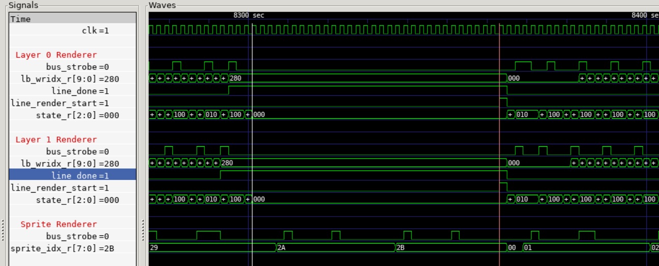
Maximum Configuration Waveform.
As you can see, both Layer Renderers reach Line Buffer index 640, i.e. the end of the scanline, about 31 cycles before the start of the next scanline.
External Bus Load on the VRAM Bus
In the simulations I’ve done, I didn’t include any load on the VRAM bus coming from the external bus. I don’t expect any issues in the Commander X16 configuration. The 65c02 CPU runs at 8MHz and can generate a load or a store instruction once every four clock cycles. That corresponds to about 12.5 25MHz clock cycles. In other words, the maximum load from the external bus on the VRAM bus is (1/12.5)x100% = 8%. The maximum load on the VRAM bus from the renderers combined is 26%+26%+13% = 65%. There’s enough bus bandwidth left for that 8% load coming from the 65c02.
In other configurations, however, e.g. when the external bus is replaced with a Wishbone slave port in an SoC, it’s a different matter entirely. That’s a topic for a future post.
The Simulation
I used BoxLambda’s build infrastructure to create a Verilator simulation model of VERA, so I could study the waveforms. I instantiated the VERA repository as a git submodule in BoxLambda and I created a vera_standalone gateware project directory, to be built in a simulation build tree.
The simulation setup, implemented in sim_main.cpp, is straightforward. These are the steps:
-
The VERA model is instantiated with the Sprite Attribute RAM preconfigured. The Sprite Attribute RAM configuration loop is implemented in the sprite_ram.v module:
for (i=(256-2*128); i<256; i=i+2) begin mem[i][11:0] = 'h100; // addr mem[i][15] = 1; // mode: 8bpp mem[i][25:16] = 10'(32*i); // x mem[i+1][9:0] = 10'd3; // y mem[i+1][16] = 0; // hflip mem[i+1][17] = 0; // vflip mem[i+1][19:18] = 2'd3; // z mem[i+1][23:20] = 0; // collision mask mem[i+1][27:24] = 0; // palette offset mem[i+1][29:28] = 2'd0; // width: 8 mem[i+1][31:30] = 2'd0; // height: 8 end - The model runs for 500 clock cycles to give the VERA synchronizer time to take the system out of reset.
-
The model is configured using register writes over the external bus. The external bus register write access is implemented in the ext_bus_wr() function in sim_main.cpp:
ext_bus_wr(VERA_DC_VIDEO, 0x71); //sprite enable, Layer 1 enable, Layer 0 enable, VGA output mode. ext_bus_wr(VERA_L0_CONFIG, 0x23); //Tile Mode, 8bpp. ext_bus_wr(VERA_L0_TILEBASE, 0x0); //tile height/width 8. ext_bus_wr(VERA_L1_CONFIG, 0x23); //Tile Mode, 8bpp. ext_bus_wr(VERA_L1_TILEBASE, 0x0); //tile height/width 8. - The model runs for 500000 clock cycles, which is enough to cover a fair number of scanlines.
- The simulation waveform is saved to file simx.fst, which can be opened with gtkwave for analysis.
I had to make a few minor modifications in the VERA code base to be able to make it build with Verilator:
- Extend the _ICARUS_ ifdefs to ICARUS_OR_VERILATOR ifdefs.
- Add a reset port to the palette_ram and sprite_ram modules, to appease the Verilator lint checker.
- Split the bidirectional external bus data port into two unidirectional ports, one input (extbus_d), and one output (extbus_dout).
- Added VERA_SPI, VERA_AUDIO, and VERA_COMPOSITE_VIDEO ifdefs to be able to include/exclude VERA’s SPI controller, audio functionality, and composite video functionality.
Try It Out
- Install the Prerequisites.
- Get the BoxLambda repository:
git clone https://github.com/epsilon537/boxlambda/ cd boxlambda - Switch to the understanding_vera tag:
git checkout understanding_vera - Set up the repository. This initializes the git submodules used and creates the default build trees:
./boxlambda_setup.sh - Build the vera_standalone project:
cd build/sim/gw/projects/vera_standalone make vera_standalone_sim - Execute the generated verilator model with tracing enabled:
./Vmodel -t - Load the generated traces into gtkwave:
gtkwave simx.fst
Thank you, Frank van den Hoef
Studying VERA was an interesting exercise. Frank van de Hoef created a very elegant retro video controller and he deserves a lot of credit for contributing its code base to the open-source community.
The next post will be about integrating VERA into the BoxLambda SoC. I’ve been looking forward to this part of the project for a long time.