The Interconnect, Harvard Architecture, and Dual Port RAM.
Updated 2 April 2026: Corrected stale links.
Updated 23 December 2025:
- Corrected link to UpdateMem and XPM Memories in documentation.
- Removed reference to ‘On WSL’ documentation.
- Fixed von Neumann and Harvard waveform diagrams.
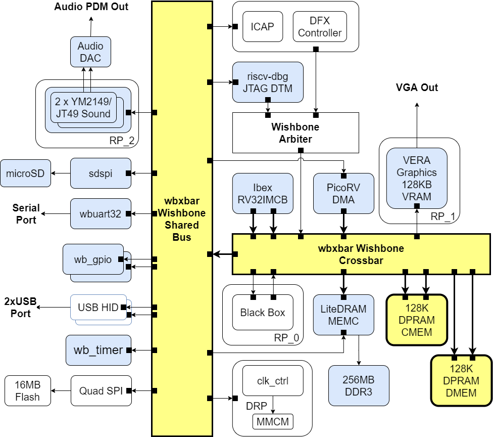
The BoxLambda Architecture Diagram with Revised Interconnect and Harvard Architecture.
When you develop in public, you make embarrassing mistakes in public. Somehow, I failed to see that after implementing the PicoRV DMA optimizations (picorv_dma_2 tag), the design no longer met the timing requirements… Yeah, I know.
I parked the task of adding keyboard and mouse support to the project and switched gears to address the timing issue. This led to the following chain of events:
- The test build with the timing issue is currently just a set of cores loosely organized along a shared bus. This is not BoxLambda’s final architecture. Rather than analyze the timing of this throwaway architecture, I should switch over to the intended architecture and analyze any timing issues in that context.
- I’ve had some architectural modifications in the back of my mind for a while. If I was going to implement the architecture, I had to bring those modifications to the foreground.
- The first change is that I wanted to use a crossbar-based interconnect instead of two shared buses.
- The second architectural change is that I wanted to move to a Harvard architecture, i.e. independent paths for instruction fetches and data accesses coming from the Ibex processor.
- As an indirect consequence, a few other changes came along, such as Word Addressing and defining the BoxLambda SoC as a component.
The result is a bit of an architectural overhaul, further discussed below.
Recap
This is a summary of the current state of affairs for BoxLambda. We have:
- An Ibex RISC-V core, Wishbone shared bus, timer, two GPIO ports, UART core, and internal memory.
- DDR3 external memory access through the Litex Memory Controller.
- OpenOCD-based Debug Access, both on FPGA and Verilator.
- VERA-based VGA graphics: 2 layers tile or bitmap mode, 2 banks of 64 sprites, 128KB Video RAM, 256 color palette.
- Dual YM2149 PSG Audio.
- SD Card Controller and FatFs File System.
- A PicoRV32-based Programmable DMA Controller.
- A Picolibc-based standard C environment for software running on the Ibex RISC-V core.
- Test builds running on Arty-A7-35T, Arty-A7-100T, Verilator, and CocoTB.
- A Linux CMake and Bender-based Software and Gateware build system with support for automated testing and post-implementation memory updates.
Crossbar and Shared Bus vs. Two Shared Buses
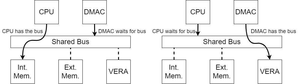
Shared Bus Interconnect Example.
In a Shared Bus architecture, only one bus Master can access the bus at a time. To allow simultaneous transactions from both the CPU and the DMA Controller, I created two shared buses in the original BoxLambda architecture: the Processor Bus and the DMA Bus.
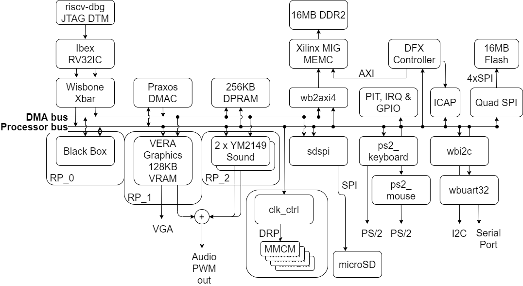
The original BoxLambda Architecture - Two Shared Buses.
This approach has some drawbacks, however:
- The CPU has two bus master ports, one for instructions, and one for data. There’s also a Black Box bus master, to be loaded onto a live system using DFX. If I want to allow simultaneous transactions from all of these bus masters, I would have to create not two, but four shared buses.
- The bus masters and key bus slaves such as VERA and LiteDRAM need ports on all of these shared buses. The bus masters have to be equipped with bus dispatchers to connect to the shared buses. The bus slaves have to be equipped with MUXes.
To avoid having to add all those buses, ports, dispatchers, and MUXes, I decided to modify the architecture and use a Crossbar Interconnect instead. A Crossbar Interconnect creates on-demand channels between bus masters and slaves and can maintain multiple such channels. A Crossbar Interconnect can accept transactions from multiple bus masters simultaneously, as long as they don’t target the same slave port. E.g. without getting in each other’s way, the CPU can access internal memory while the DMA controller moves data from external memory to VERA.
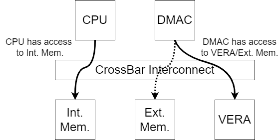
Crossbar Interconnect Example.
WBXBAR
I’m using ZipCPU’s WBXBAR module as the CrossBar for BoxLambda:
https://github.com/ZipCPU/wb2axip/blob/master/rtl/wbxbar.v
The WBXBAR Crossbar is well-documented in this ZipCPU Blog post:
https://zipcpu.com/blog/2019/07/17/crossbar.html
Crossbar and Shared Bus
The size of a Crossbar Interconnect increases quickly with the number of ports, however. A NxN square Crossbar has N^2 nodes. If I put all bus masters and slaves on a single WBXBAR instance, the Crossbar uses 5717 LUTs and 2505 Slice Registers. As a compromise, I put the slow slaves on a Shared Bus and attached that bus to a Crossbar Interconnect consisting of bus masters and fast slaves (read: memories). In this configuration, the entire interconnect requires 2846 LUTs and 2022 Slice Registers.
| Interconnect Configuration | LUTs | Slice Registers | |
|---|---|---|---|
| Single 6x21 Crossbar | 5717 | 2505 | |
| 5x8 + 1x14 + 2x1 Crossbar | 2846 | 2022 |
The resulting configuration looks like this:
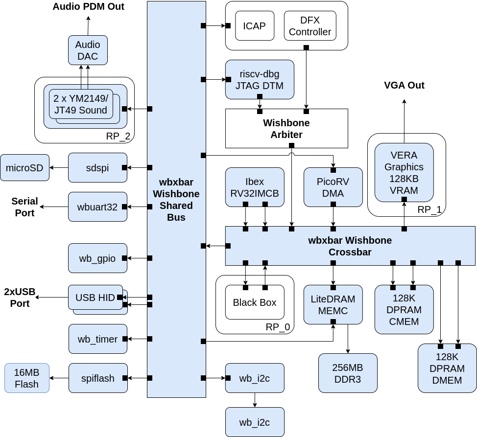
Revised BoxLambda Architecture - Arty A7-100T Configuration.
Note that the shared bus is just another WBXBAR instance. A crossbar instance with one bus master port is equivalent to a shared bus instance with one bus master port.
Two Dual Port Memories
In the modified BoxLambda Architecture I replaced the single Dual Port memory instance with two Dual Port instances: CMEM and DMEM. The two instances create a Harvard Architecture (see below). The RAMs are Dual Port to allow simultaneous memory access from both the CPU and the DMA Controller.
Harvard vs. Von Neumann
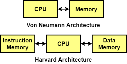
Harvard vs. Von Neumann Architecture.
In a Von Neumann Architecture, the CPU has access to one memory that stores both instructions and data. Instruction Fetch and Data Access transactions share one memory bus. In a Harvard Architecture, Instruction Memory is separate from Data Memory. Instruction Fetch and Data Access transactions can be executed independently.
The Ibex processor has separate Instruction and Data ports. In the original BoxLambda architecture, both ports were connected to a shared bus, effectively creating a Von Neumann Architecture. In such a configuration, the waveform of a word copy operation looks like this:
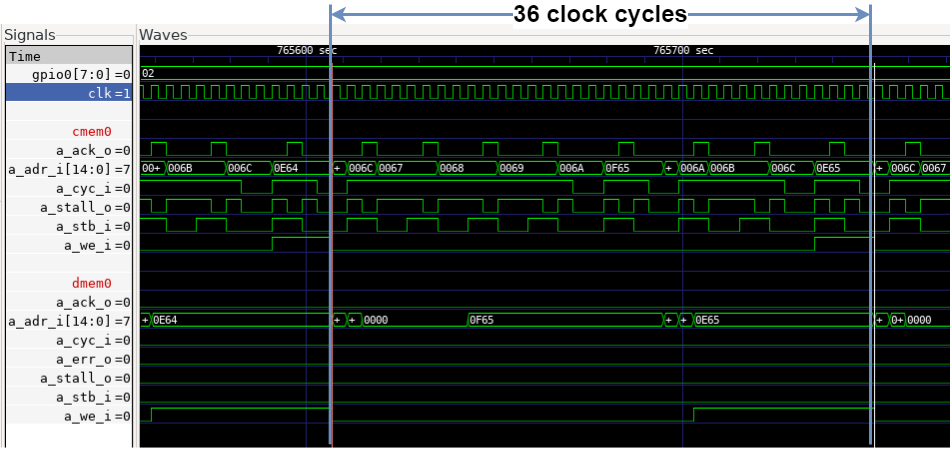
Word Copy in Von Neumann Architecture.
Both instruction fetches and data accesses go to the same port. Due to the interleaving of instructions and data, it takes 36 clock cycles to copy one word.
By contrast, if you connect the Instruction and Data Ports to two separate memories via a Crossbar Interconnect, the waveform of a word copy operation looks like this:
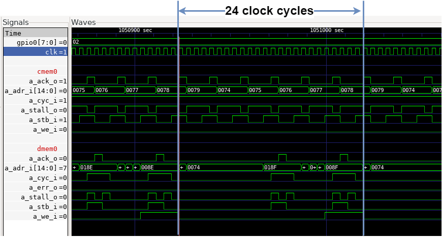
Word Copy in Hardvard Architecture.
Instruction fetches go to CMEM port 0. Data accesses go to DMEM port 0. In this configuration, it takes 24 clock cycles to copy one word. That’s a 33% performance improvement.
The Dual-Port RAM Modules
A wb_dpram_wrapper.sv module selects one of two DPRAM implementations depending on whether we’re targeting simulation or FPGA synthesis.
On FPGA, I’m using an XPM_MEMORY_TDPRAM instance. Using an XPM macro for internal memory allows me to do post-synthesis memory image updates in the bitstream file, as described here.
Here is the XPM_MEMORY_TDPRAM documentation:
https://docs.xilinx.com/r/en-US/ug974-vivado-ultrascale-libraries/XPM_MEMORY_TDPRAM
I did run into a spurious write issue with XPM_MEMORY_TDPRAM. To avoid the issue, I had to qualify the Write Enable (wea/web) signals with the valid signals even though the valid signals were already going to the module’s Memory Enable ports (ena/enb):
    assign a_valid    = a_cyc_i & a_stb_i;
    assign b_valid    = b_cyc_i & b_stb_i;
    ...
    assign a_ram_we   = {4{a_we_i&a_valid}} & a_sel_i;
    assign b_ram_we   = {4{b_we_i&b_valid}} & b_sel_i;
    ...
    .ena(a_valid),                       // 1-bit input: Memory enable signal for port A. Must be high on clock
                                        // cycles when read or write operations are initiated. Pipelined
                                        // internally.

    .enb(b_valid),                       // 1-bit input: Memory enable signal for port B. Must be high on clock
                                        // cycles when read or write operations are initiated. Pipelined
                                        // internally.
    ...
    .wea(a_ram_we),                     // WRITE_DATA_WIDTH_A/BYTE_WRITE_WIDTH_A-bit input: Write enable vector
                                        // for port A input data port dina. 1 bit wide when word-wide writes are
                                        // used. In byte-wide write configurations, each bit controls the
                                        // writing one byte of dina to address addra. For example, to
                                        // synchronously write only bits [15-8] of dina when WRITE_DATA_WIDTH_A
                                        // is 32, wea would be 4'b0010.

    .web(b_ram_we)                      // WRITE_DATA_WIDTH_B/BYTE_WRITE_WIDTH_B-bit input: Write enable vector
                                        // for port B input data port dinb. 1 bit wide when word-wide writes are
                                        // used. In byte-wide write configurations, each bit controls the
                                        // writing one byte of dinb to address addrb. For example, to
                                        // synchronously write only bits [15-8] of dinb when WRITE_DATA_WIDTH_B
                                        // is 32, web would be 4'b0010.
    ...
In simulation, I’m using Alex Forencich’s wb_dp_ram.v module.
Link Script Changes
The new memory organization required some Link Script changes:
- For the Arty A7 100T configuration, the amount of internal memory set aside for data is smaller than before. 128 KB vs. 192 KB. For some SW builds I was running out of heap memory as a result. To fix this, I mapped the heap to external memory, of which we have plenty.
- I created a .cmem_bss section, mapped to CMEM, so it is still possible to put data in CMEM by assigning it to this section.
/*Create some data buffers in CMEM by mapping them to the .cmem_bss segment.*/ char cmem_str[32] __attribute__ ((section (".cmem_bss"))); - Similarly, I created a .dmem_text section so code can still be put in DMEM if needed.
/*This function executes from DMEM.*/
__attribute__ ((section(".dmem_text")))
int code_in_dmem(char *message) {
  int i, j;
...
Dual Port RAM Test
I added a test build, gw/projects/dual_port_ram_test/ to verify access to the dual port memories. The test program checks instruction and data access to both of the memories. The program also includes a test exercising both ports of the Dual Port RAM simultaneously. One port is accessed by the CPU, and the other port by the DMA Controller.
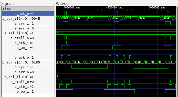
Both DPRAM ports being accessed simultaneously.
Other Changes
Word Addressing
The previous BoxLambda test SoCs contained a combination of Byte Addressing and Word Addressing bus masters as well as a combination of Byte Addressable and Word Addressable slaves. Add four Byte Enable signals to that picture and things can get pretty confusing. To avoid this ambiguity and confusion, I switched everything over to Word Addressing. BoxLambda now uses a 28-bit Word Address Bus.
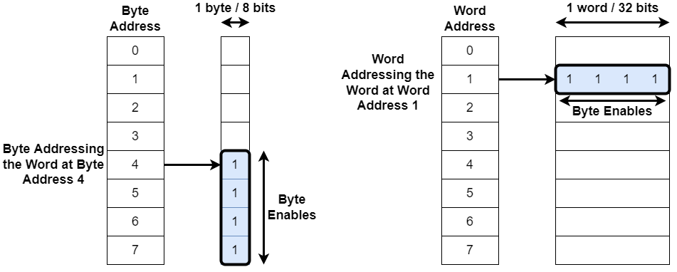
Byte Addressing (left) vs. Word Addressing (right).
Note that you can still address a byte using a Word Addressing bus. That’s what the Byte Enables are for:
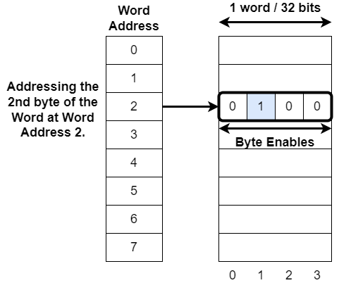
Addressing a byte using Word Addressing and Byte Enables.
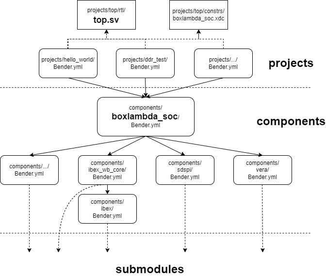
BoxLambda SoC as a Component
So far, each gw/project/ build defined its own Test SoC. Each new Test SoC copied the previous one and added its own logic so I ended up with a progression going from very simple SoCs (hello_world) to very complete SoCs (picorv_dma_sys_test).
Going forward, I’ll be maintaining just one SoC module:
gw/components/boxlambda_soc/rtl/boxlambda_soc.sv.
/*The parameterized BoxLambda SoC.*/
module boxlambda_soc #(
    parameter DPRAM_BYTE_ADDR_MASK = 'h1ffff, /*DPRAM size as a mask value. Used both from CMEM and DMEM.*/
    parameter VRAM_SIZE_BYTES = 131072,
    parameter DEBUG_MODULE_ACTIVE = 1,
    parameter DRAM_ACTIVE = 1,
    parameter VERA_ACTIVE = 1,
    parameter SDSPI_ACTIVE = 1,
    parameter YM2149_ACTIVE = 1,
    parameter PICORV_ACTIVE = 1,
    parameter CMEM_FILE = "",
    parameter DMEM_FILE = ""
    ) (
    input  wire       ext_clk_100, //100MHz external clock.
    input  wire       ext_rst_n,   //External reset pin.

`ifdef VERILATOR
  /*These JTAG signals are not used on FPGA (they are used in simulation).
   *On FPGA, the JTAG signals are driven by a BSCANE2 primitive inside the jtag tap module dmi_bscane_tap.sv.
   */
    input  wire       tck,
    input  wire       trst_n,
    input  wire       tms,
    input  wire       tdi,
    output wire       tdo,
`endif
    output wire       pll_locked_led, //PLL locked indication.
    output wire       init_done_led, //LiteDRAM initialization done indication.
    output wire       init_err_led, //LiteDRAM initialization error indication.
`ifdef SYNTHESIS
    /*The simulation build doesn't export DDR pins.*/
    output wire [13:0] ddram_a,
    output wire [2:0] ddram_ba,
    output wire ddram_ras_n,
    output wire ddram_cas_n,
    output wire ddram_we_n,
    output wire ddram_cs_n,
    output wire [1:0] ddram_dm,
    inout  wire [15:0] ddram_dq,
    inout  wire [1:0] ddram_dqs_p,
    inout  wire [1:0] ddram_dqs_n,
    output wire ddram_clk_p,
    output wire ddram_clk_n,
    output wire ddram_cke,
    output wire ddram_odt,
    output wire ddram_reset_n,
`endif
    // VGA interface
    output wire  [3:0] vga_r,
    output wire  [3:0] vga_g,
    output wire  [3:0] vga_b,
    output wire        vga_hsync,
    output wire        vga_vsync,
    // SDSPI interface
    output wire  sdspi_cs_n,
    output wire  sdspi_sck,
    output wire  sdspi_mosi,
    input  wire	 sdspi_miso,
    input  wire  sdspi_card_detect_n,
    // Audio interface
    output wire       audio_out,
    output wire       audio_gain,
    output wire       audio_shutdown_n,
`ifdef VERILATOR
    // Audio interface signals only used in simulation
    output wire [15:0] pcm_out,
    output wire acc1_overflow,
    output wire acc2_overflow,
`endif
    // UART and GPIO
    input  wire       uart_rx,
    output wire       uart_tx,
    inout  wire [7:0] gpio0,
    inout  wire [3:0] gpio1
    );
Different gw/project/ builds still exist. They just differ in the way they instantiate boxlambda_soc, including or excluding specific subcomponents. Most gw/projects reference the same top.sv, but with a different combination of defines in their Bender.yml manifest.
Build Diagram with BoxLambda SoC component and top.sv.
Gw/project/ builds also differ in the software program they run on the SoC. This is specified in the gw/project/’s CMakefile.
Try It Out
Setup
- Install the Software Prerequisites.
- Get the BoxLambda repository:
git clone https://github.com/epsilon537/boxlambda/ cd boxlambda - Switch to the interconnect tag:
git checkout interconnect - Set up the repository. This initializes the git submodules used and creates the default build trees:
./boxlambda_setup.sh
Dual Port RAM Test on Verilator
- Build the dual_port_ram_test project:
cd build/sim-a7-100/gw/projects/dual_port_ram_test make dual_port_ram_test_sim_sw - Execute the generated Verilator model. You should see the following output:
./Vmodel
...
Executing code from DMEM...
CMEM word copy...
DMEM word copy...
Hello CMEM!
Load PicoRV Program wordcopy_burst
Taking PicoRV out of reset...
Dual copy from DMEM to CMEM...
Dual copy from CMEM to DMEM...
Test Successful.
Dual Port RAM Test on Arty A7
- Connect a terminal program such as Putty or Teraterm to Arty’s USB serial port. Settings: 115200 8N1.
- Build the project in an Arty A7 build tree (arty-a7-35 or arty-a7-100):
cd build/arty-a7-100/gw/projects/dual_port_ram_test make dual_port_ram_test_bit_sw - Download the generated bitstream file to the Arty A7:
make dual_port_ram_test_load - In the Putty terminal, you should see the same output as with the Verilator test build above.
Conclusion
After all this refactoring, I still had two timing violations:
- a setup violation in the return data path from the PicoRV DMA’s Program memory to the Wishbone slave port. I fixed this issue by inserting a register stage in the sys_clk clock domain.
- a setup violation in the return data path from the Wishbone bus master port to the PicoRV. I fixed this issue by inserting a register stage in the PicoRV’s sysclkx2 clock domain.
Every significant project I’ve worked on over time accumulates tasks that I consider important but not urgent. These tasks often get deferred because they are mostly non-functional improvements. They don’t add features. Invariably, however, there comes this point where these tasks no longer let themselves be deferred. They have to be tackled before further progress can be made. The planned work grinds to a halt for a while as I process these now-blocking tasks. The result is usually an overhaul. When done, barring any regressions, the system still does the same things as before. It just does it better and I’m in a good position again to add new functionality.